Where does one start after so long an absence — meaning only the blog abstinence; I have been working and publishing since last time;-)  One of the things which have been on my mind is the ideality factor, a figure of merit for the charge carrier recombination mechanism in a semiconductor diode. In short, a diode ideality factor of 1 is interpreted as direct recombination of electrons and holes across the bandgap. An ideality factor of 2 is interpreted as recombination through defects states, i.e. recombination centres. More on that in a later post, let’s start with the basics.
A couple of years ago, I wrote about some general properties of current-voltage characteristics of organic solar cells, but did not describe the ideality factor.1 I think the ideality factor was mentioned only once, and then without details.
The Shockley diode equation describes the current–voltage characteristics of a diode,
 .
.
Here,  current,
  the voltage,
  elementary charge,
  thermal voltage,
  the dark saturation current, and
  the photogenerated current. If the ideality factor
  was equal to one, one could call this the ideal Shockley equation. It derivation can be found in semiconductor text books, but it can also be derived based on thermodynamic arguments (see Peter Würfel’s excellent book on the physics of solar cells).
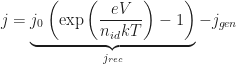
The current flowing out of the diode is defined to be negative. Essentially, the charge carriers which can flow out are the generated ones (e.g. ), but reduced by the recombination current. That means,
 .
.
However, the term  contains also a negative contribution, times the
  from the bracket. This is the thermal generation current
  , i.e. charge carriers excited across the bandgap just by thermal energy — and therefore very little. Still, the term is very important, as it is the prefactor of the whole
  curve. Without light, i.e. with photocurrent
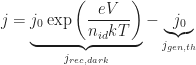
  , we can clarify
 .
.
so that at negative voltages,  .
.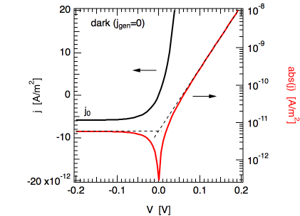 (Please note that under realistic conditions, is not only pretty small and difficult to measure in principle, it is also hidden behind shunt currents in the device. ) At zero volt,
  . Thus, generation = recombination — or more specifically, thermal generation current = recombination current — which essentially implies that 0V correspond to the open circuit voltage in the dark.
How can one determine the ideality factor and the dark saturation current (at least in principle, see below for a better way on real devices)? It is common to neglect the thermal generation current (the term -1, multiplied by ), which is a good approximation for voltages some  larger than 0. Then, calculate the logarithm of the dark current (),
 ,
,
so that the ideality factor can be determined from the inverse slope of the ln(current) at forward bias, and the dark saturation current from the current-axis offset. Let me already tell you that I do not recommend this approach, for reasons written below, and as explained in more detail in a recent paper of Kris Tvingstedt and myself [Tvingstedt/Deibel 2016].
Under illumination and at open circuit conditions,  , we can rewrite the Shockley equation as
 ,
,
which has the same shape as the Shockley equation in the dark. This means that if you measure ( ) pairs for a (wide) range of different illumination intensities (thus varying ), the points should overlap with the dark curve! We’ll come back to this important point further below. Note that for solar cells with good fill factor, can be approximated by the short circuit current
  . Continue reading “The diode ideality factor in organic solar cells: basics”


 This time I want to show you that a plot that is very common in today’s literature does not make much sense for today’s high-efficiency organic solar cells. I am talking about the plot of photocurrent – the difference between illuminated and dark current of a solar cell – vs what is called “effective voltage”, i.e.,


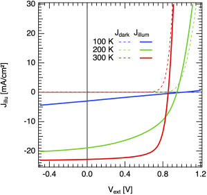


 mainly for doing device simulations with Rod’s
  The ideal diode equation was discussed with respect to the ideality factor in
  ,
, the recombination ideality factor,
  the photogenerated current. For simplicity, the latter is chosen to be voltage independent, and therefore is equal to the short-circuit current
  .
. , we get
 ,
, .
. is the photocurrent due to solar illumination, and the dark saturation current density
  – we see that
  , too. Generally, the thermal generation leading to
  .
.
 . The result could look like the scheme shown in the figure below. I have adapted this figure from Maria’s new publication on transport resistance losses in organic solar cells [
 curve (blue) is the normal JV curve under illumination, where
  is the applied voltage. The down-shifted suns-Voc curve corresponds to the
  (red); the implied voltage is the voltage without any series-resistance imposed drops. In other words, the externally applied voltage drops over the diode and all series resistances, the external series resistance as well as the transport resistance that comes from a low active layer (or transport layer) conductivity. The implied voltage, as measured by the open-circuit voltage (at zero current, where series resistances do not play a role), corresponds to the voltage without drops over series and transport resistance.
 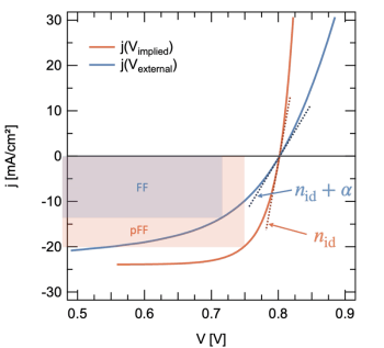 If a solar cell has a low active layer conductivity and is transport resistance limited, than the measurement of the suns-Voc curve to construct the

 Just as brief progress indicator, here a
  I moved from Würzburg to the Institute of Physics at

