In one of my last posts on the diode ideality factor (6 years ago…), I promised to talk about the transport resistance in organic solar cells.  I came across it already during my time at IMEC in Leuven, Belgium, around 2004: my colleagues and I worked on an analytic model of the open circuit voltage in organic bilayer solar cells. The corresponding paper was published a few years later, [Cheyns et al 2008], but I have to admit that I did not grasp its importance as a relevant loss mechanism for organic solar cells in general, focussing on geminate and nongeminate recombination – until this paper by [Würfel/Neher et al 2015] came out. I think now I have;)
The transport resistance is an internal resistance in the active layer (or transport layer(s)) of the solar cell, acting like an internal series resistance: It changes the slope of the current density–voltage characteristics – for instance around the open circuit voltage – and thus reduces the fill factor.
If you can live with an effective conductivity  for now, I’d say that the transport resistance is given as
with the effective carrier concentration  , the effective mobility
  , and the active layer thickness
  . For a finite current
  , the externally applied voltage
  of the
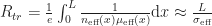
  curve (red in the sketch)
  - contributions to current-voltage characteristics - variation 2.png") is reduced by
is reduced by  as compared to the transport resistance free case which I call
  (violet). The reason is that the electron and hole energy levels equivalent to conduction and valence band are more tilted due to the influence of the low conductivity. Rod MacKenzie from Durham used his drift–diffusion simulation programme gpvdm – which among many other features allows to use the multiple-trapping-and-release model to account for energetic disorder – to calculate an example. In the figure, the energy levels corresponding to conduction and valence band are shown, and the yellow shading between the band edges correspond to the trap populations which I will ignore. So focus on the edges!
  The upper left inset features the band bending of the transport resistance free case at a current–voltage point in the fourth quadrant of an illuminated solar cell,
  being at 0.8 V. The red lines show that in the bulk, the bands are perfectly flat despite not being at any “flat band” voltage. In contrast, the lower left inset shows the band bending for the illuminated current–voltage point at the same current, but at of 0.69 V. The voltage difference
  of 0.11 V is due to the transport resistance. The two perfectly horizontal red lines, just shifted down from above, now show a discrepancy due to the band bending in the bulk. This tilt sums up to the voltage loss , and corresponds to a gradient of the quasi-Fermi levels, as discussed clearly in [Würfel/Neher et al 2015] around Eqn (8). Let me note that the denomination of as opposed to is a bit unfair, as the latter still drops across the whole (active) layer thickness – but the gradient is different. So, can the two different band bendings (upper left and upper right) occur at the same time? No of course not. The lower right shows you how a simulated organic solar cell with realistic parameters looks inside: it is limited by a transport resistance due to low effective conductivity in the active layer, which shows up as tilt in the bands, and implies a gradient in the quasi-Fermi levels. The upper right shows you how the bands looked if the solar cell were not limited by a transport resistance (and how they do look under the special case of open circuit conditions).
Still, the voltage drop due to the transport resistance – coming from the low conductivity and leading to the tilted transport levels – is real and does reduce the fill factor.
In my recent talk at the MRS Spring meeting (invited! in person! on Hawaii! slides here:), I showed the approximate difference of the internal and external voltage of a fresh, inverted PM6:Y6 bulk heterojunction solar cell ( = 200 nm, but qualitatively similar for 100 nm) at different light intensities, from 3 micro-suns to 1 sun (300 nW/cm2 to 100 mW/cm2).  The ideal diagonal case where
  is only seen for the lowest light intensities. In contrast, at 1 sun illumination, when 0.4 V are applied, the internal voltage is still at around 0.7 V. The fill factor at 1 sun is, by the way, somewhat above 60%, whereas the transport resistance free pseudo fill factor (determined using the Suns-Voc method, see below) is above 80%. As If you are interested in the details of this study, please have a look at our preprint. [Update 2022-07-01]: now published in Nature Communications.
How did we determine the approximate internal voltage, or , when we only have direct access to the external (i.e., applied) voltage? Similar to [Schiefer et al 2014], we used the Suns-Voc method as a measure for the series and transport resistance free current–voltage characteristics. The idea is in the post on the diode ideality factor, but before sending you away again I repeat it here: the current density, as given by the diode equation under assumption of the superposition principle,
 (*)
(*)
is influenced by the series resistance  and parallel resistance
  . At open circuit,
  , the current
  is zero,
 ,
,
so that the terms including the series resistance (but not the parallel resistance!) become zero as well. Reordering the equation,
 ,
,
we have an equation very similar to the diode equation (*). The pairs  measured under a wide range of light intensities can, when shifted down by
  , correspond to the so called Suns-Voc curve. It represents the curve, as the open circuit voltage is transport resistance free so that (only) there,
  . The Suns-Voc curve is equivalent to the illuminated curve, but lacks the influence of the series and transport resistance. The generation current
  with the generation rate
  is sometimes (ok, often..) approximated by the short circuit current
  .
.
An example of how a Suns-Voc curve looks is shown in my earlier post on the diode ideality factor in the third figure (red = illuminated  ), green symbols = Suns-Voc curve).
Of course there is a better way by measuring both the voltage dependent current and luminescence of a solar cell, as done by [Rau et al 2020] on Cu(In,Ga)Se2 solar cells: from the luminescence, which depends on the quasi-Fermi level splitting, the internal voltage can be determined. For organic solar cells, as singlet and charge transfer exciton photoluminescence need to be separated – the internal voltage will be proportional to the latter – this is harder and has not been done yet, as far as I know.
How can the impact of the transport resistance on the fill factor, and thus performance, of organic solar cells be minimised? To reduce the transport resistance, the active layer conductivity needs to be increased. This can be done by, either, increasing the charge carrier mobility – for a molecular hopping system this means reducing static (low  ) and/or dynamic disorder (low
  ). Or, increasing the carrier concentration – e.g. by doping, which is kind of hard in a bulk heterojunction, but starting with the material phase with the lower conductivity could be a viable approach.
Some hat tips here beyond the very nice cooperation of our study: Maria and Rod for feedback to an earlier version of the post, and Julien for being the first commenter on it:)


 If a solar cell has a low active layer conductivity and is transport resistance limited, than the measurement of the suns-Voc curve to construct the


 For a selection of devices that we characterised for [Saladina 2025], we show on the right-hand-side the impact of transport resistance on the fill factor. The upper limit of the FF (solid line) can be reached when the recombination ideality is unity and there are no transport resistance losses. The FF (open circles) is often much lower, but in modern devices such as PM6:Y6 it can exceed 75%. The pseudo-FF (filled circle), however, is much closer to the upper limit, and is due to the trap-assisted recombination found in organic solar cells, at ideality factors that are often larger than unity. All in all, the largest loss for the fill factor is the transport resistance loss, essentially the difference between the pseudo-FF and the FF, even for the (not shown here) record-efficiency organic solar cell devices! I believe it makes a lot of sense to quantify the transport resistance in all publications that present the performance organic solar cells, so to avoid drawing wrong conclusions – for instance, that a given low fill factor is due to recombination, when the FF loss is likely dominated by low active layer conductivities. This is even more important when looking at the losses of organic solar cells with thicker active layers.


 is changing with time during the measurement – no matter if the method is a large signal (OCVD) or small signal method (TPC, IMVS):
 – and the second term a contribution coming from the response of charge due to the measured signal of the experimental technique: the time variation of the voltage as response to a time dependent light signal (pulsed or modulated). If the latter capacitive term becomes dominant, the recombination lifetime cannot be determined anymore, as is hidden behind the RC time.
 vs
vs 
 is the
  is the voltage dependent capacitance, which can be estimated (as lower bound) by the geometric capacitance of the active layer,
  , with the dielectric constants (relative and vacuum) and
  3). The generation current density can be approximated, in most cases, by the short circuit current density
  and
and 
 after Kiermasch 2018, compared to the measured time constants by IMVS,
  . Except for, maybe, low temperatures, the RC times dominate the measured signal at high open circuit voltages, whereas the shunt limits the lifetime determination at lower open
 .
. the voltage,
  elementary charge,
  thermal voltage,
  the dark saturation current, and
  the photogenerated current. If the ideality factor
 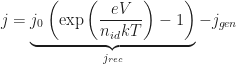 .
. contains also a negative contribution,
  from the bracket. This is the thermal generation current
  , i.e. charge carriers excited across the bandgap just by thermal energy — and therefore very little. Still, the term is very important, as it is the prefactor of the whole
  curve. Without light, i.e. with photocurrent
  , we can clarify
 .
. .
. (Please note that under realistic conditions,
  . Thus, generation = recombination — or more specifically, thermal generation current = recombination current — which essentially implies that 0V correspond to the open circuit voltage in the dark.
 ,
, , we can rewrite the Shockley equation as
 ,
, ) pairs for a (wide) range of different illumination intensities (thus varying
 and holes
  are photogenerated pair wise, the respective excess charge carrier concentrations are symmetric,
  . Then a recombination rate
 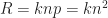 ,
, could be a Langevin prefactor – more on that later. In a transient experiment with a photogenerating, short laser pulse at
  , the continuity equation for charge carriers (here, e.g. electrons) under open circuti conditions (no external current flow, for instance if the experiment is done on a thin film without electrodes)

 (as the generation was only at


